Used VEECO / SLOAN DEKTAK 3ST #293725380 for sale
URL successfully copied!


Tap to zoom
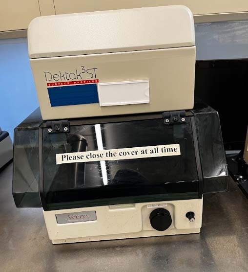

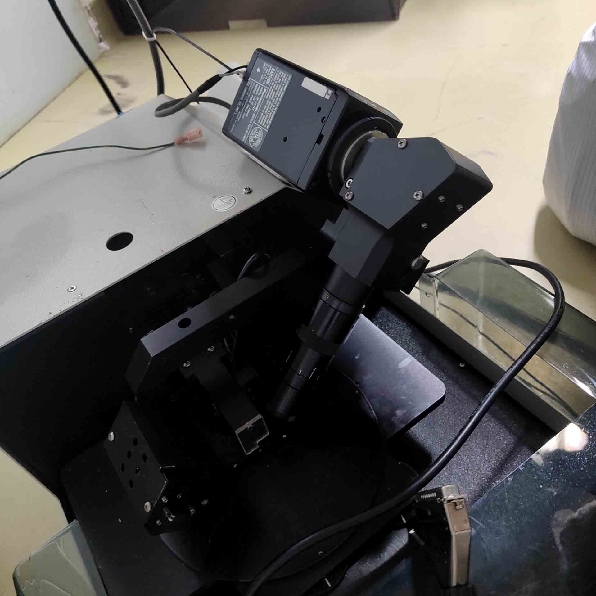
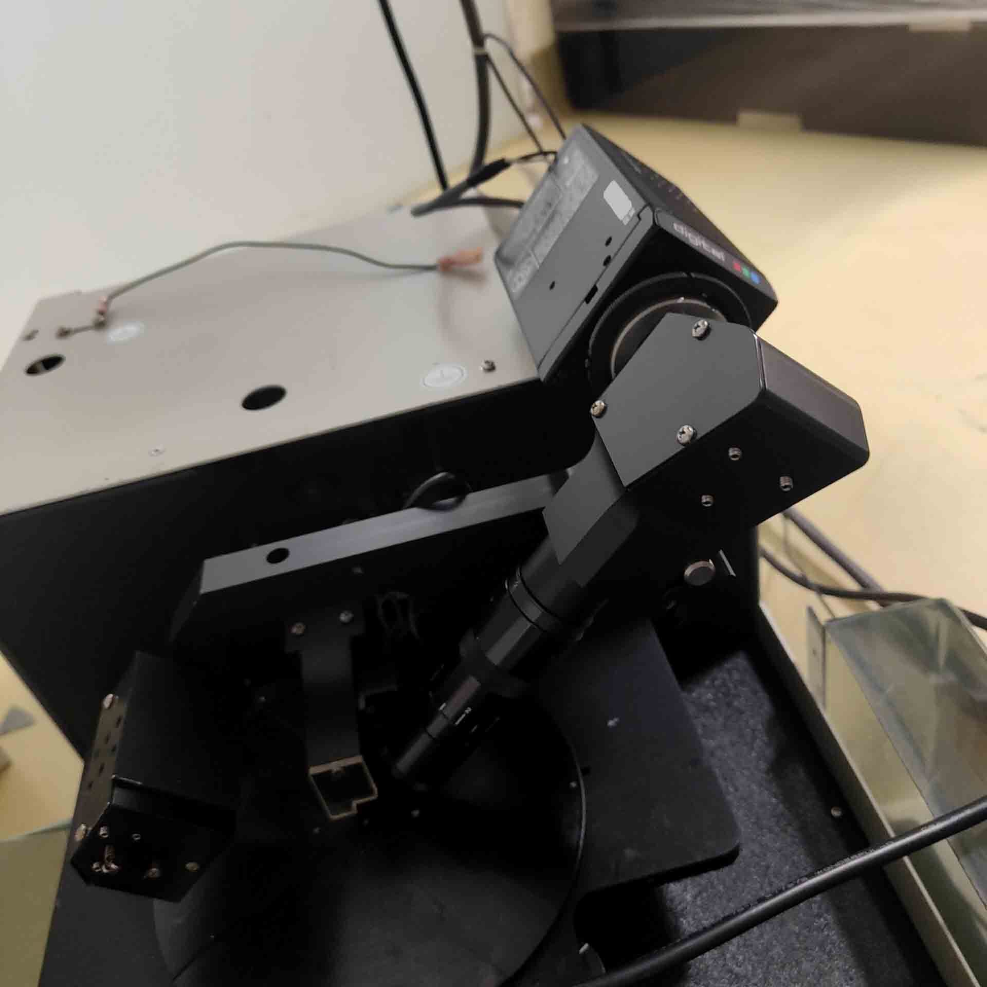
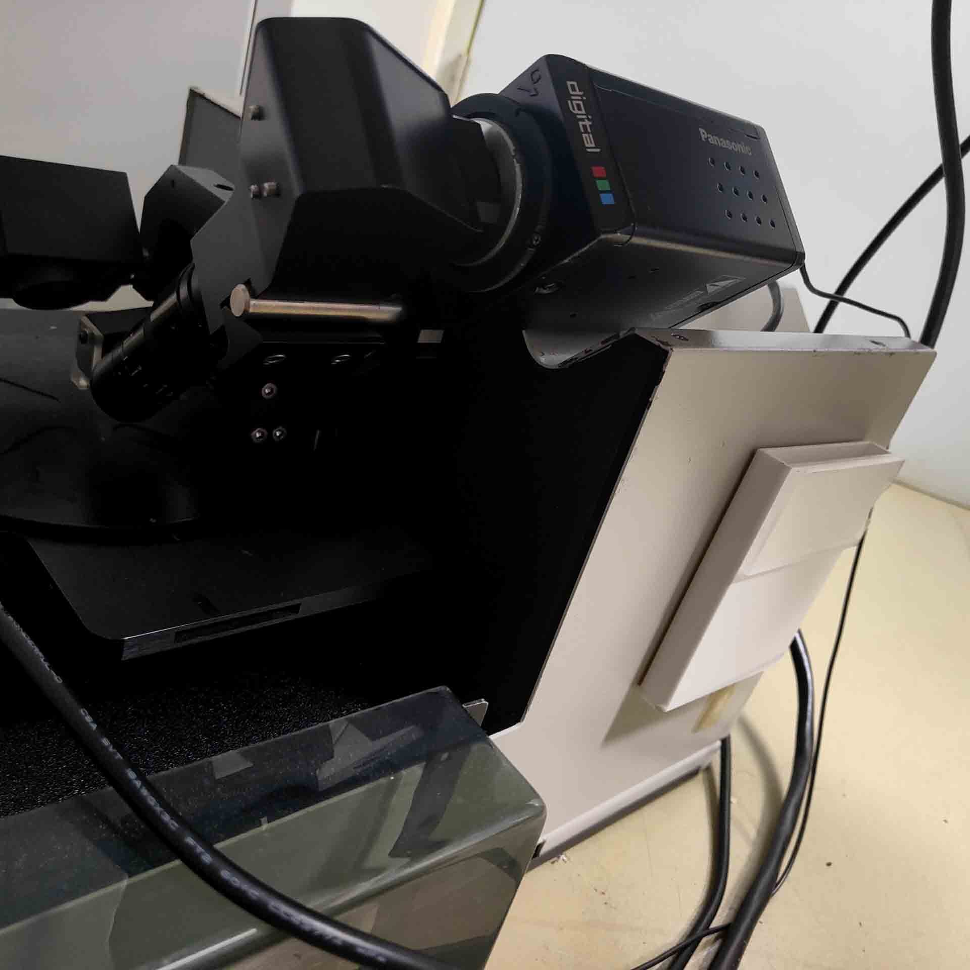
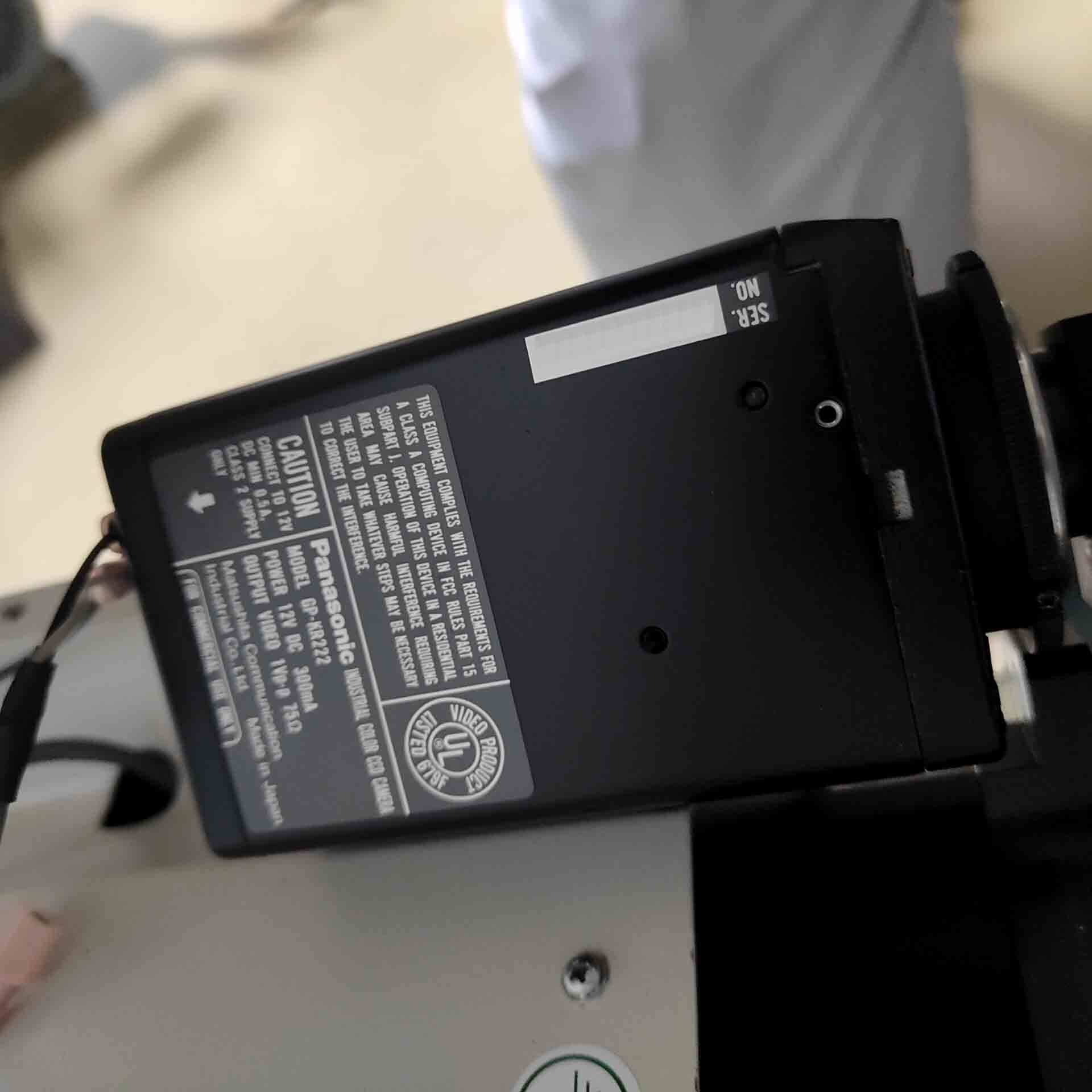
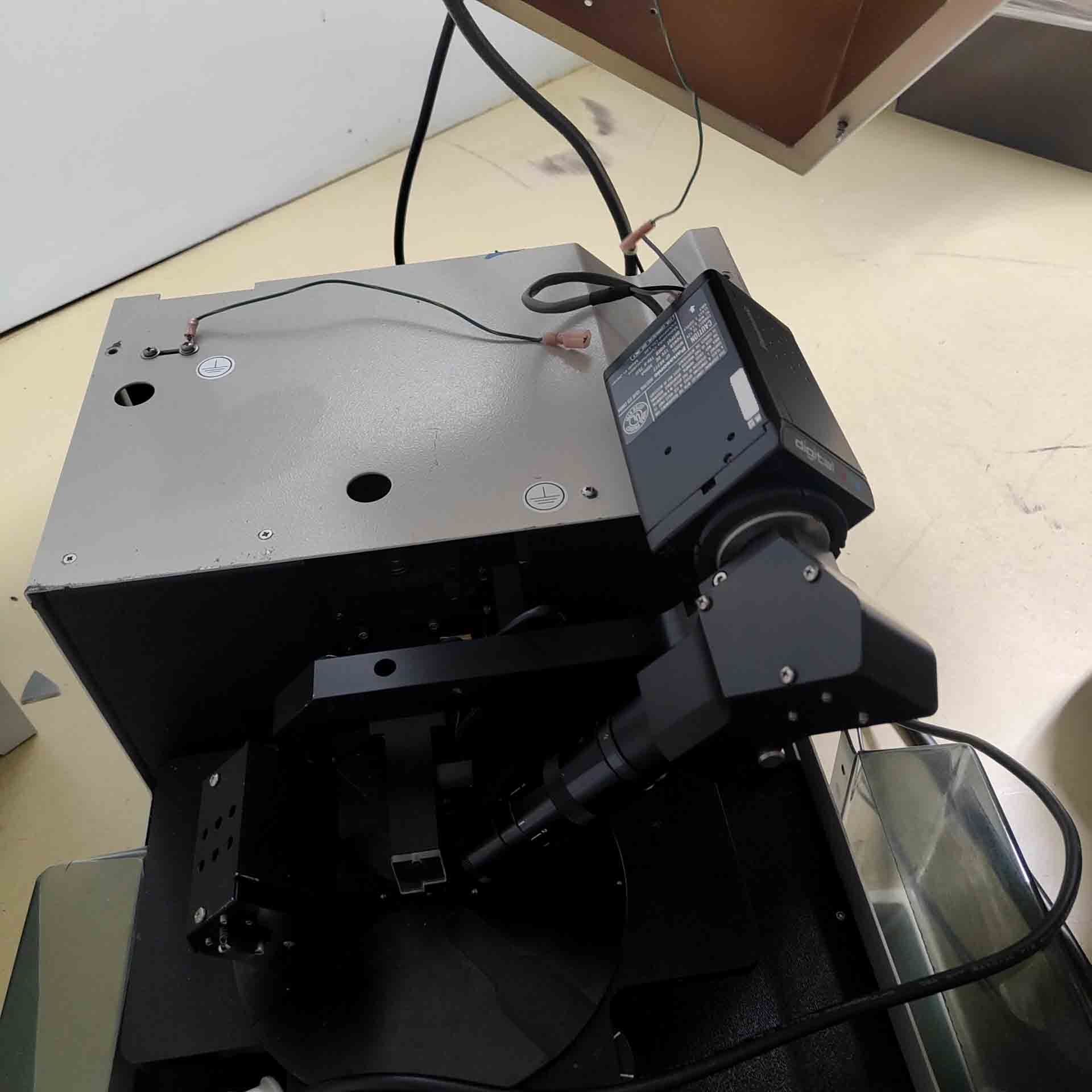
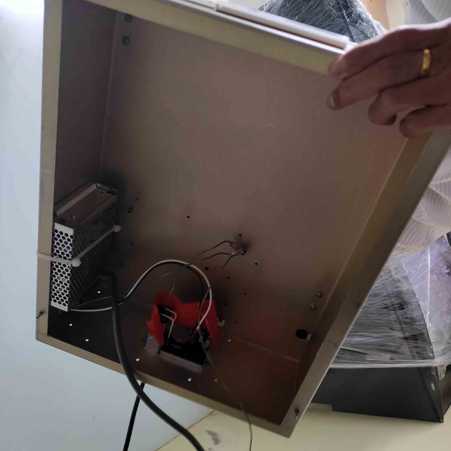
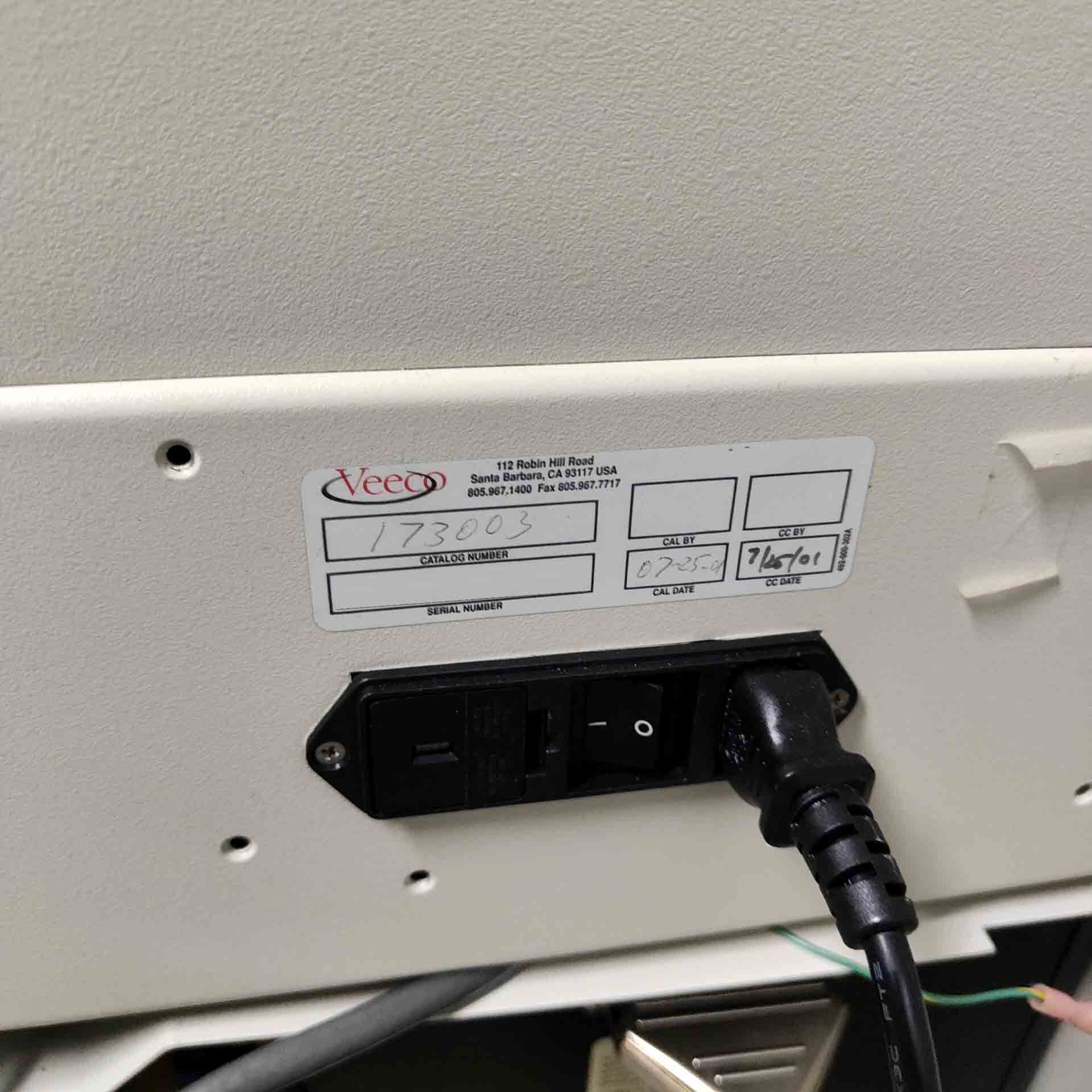
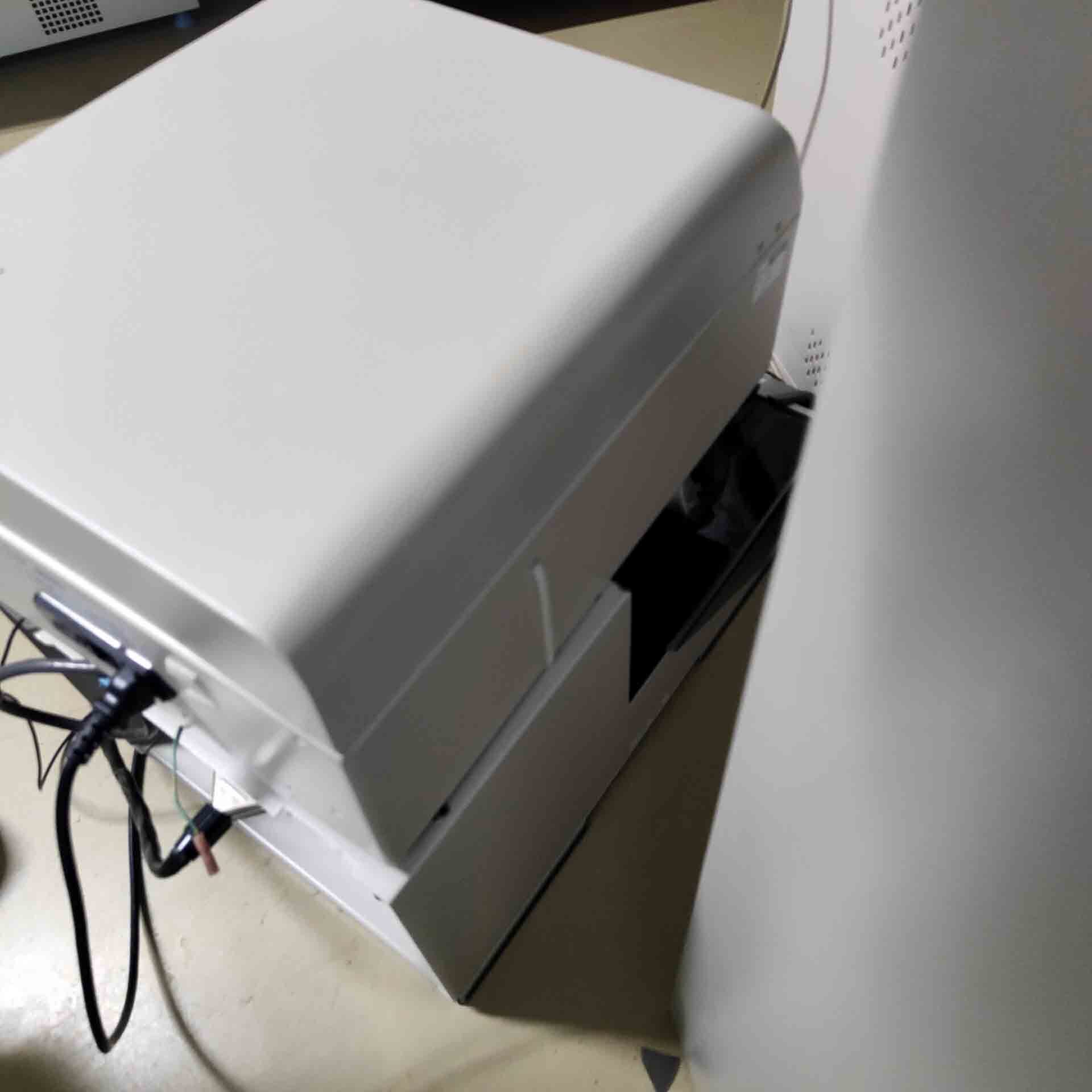
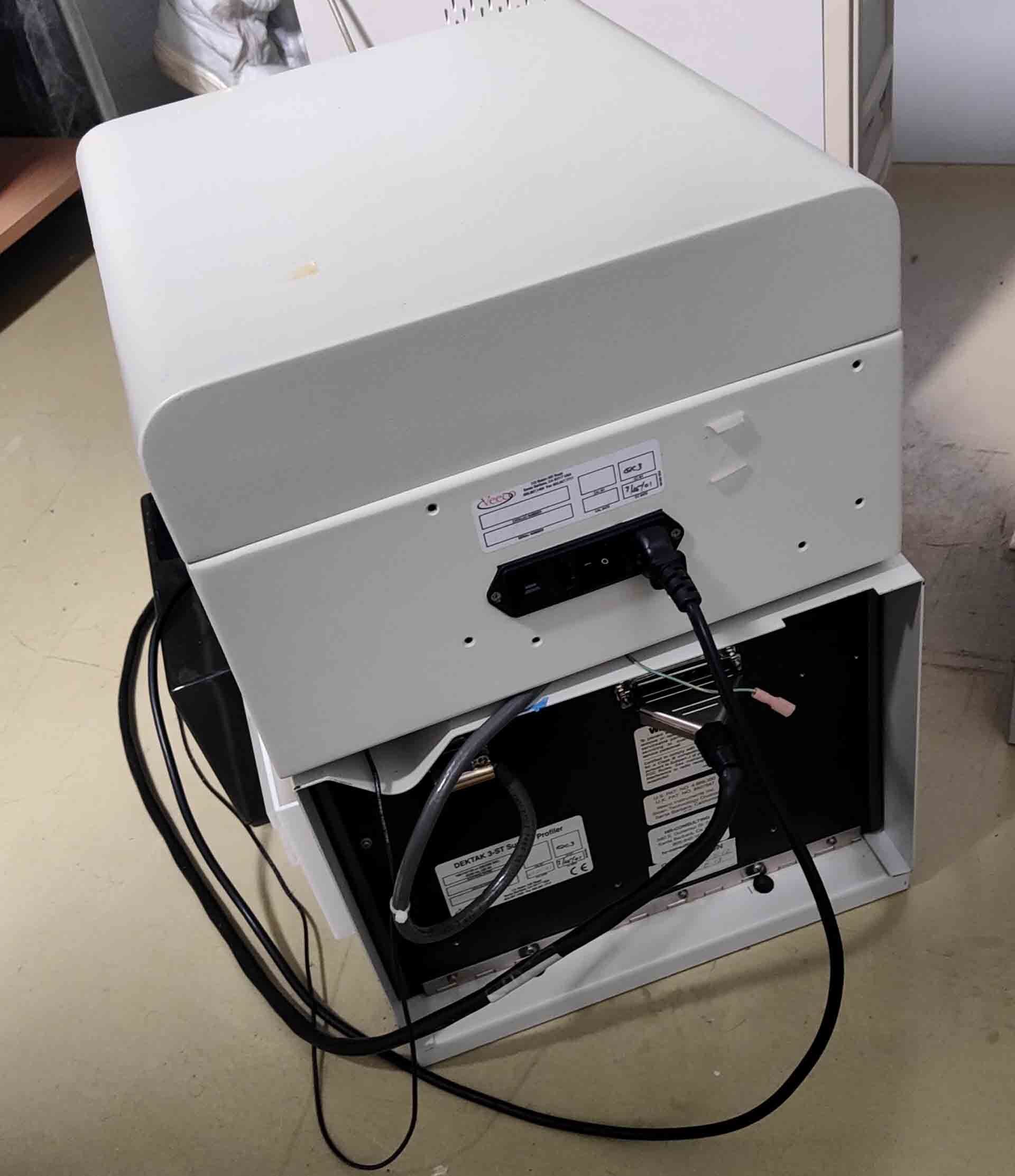
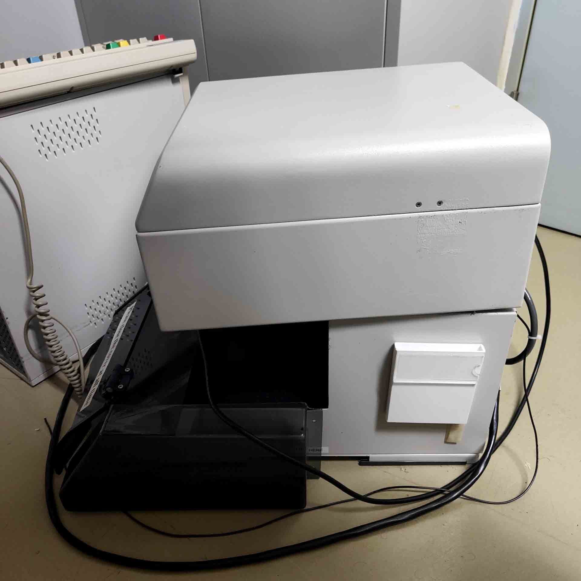
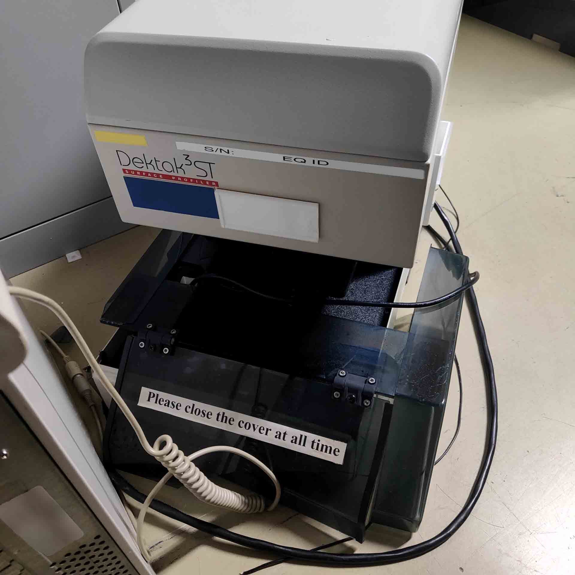
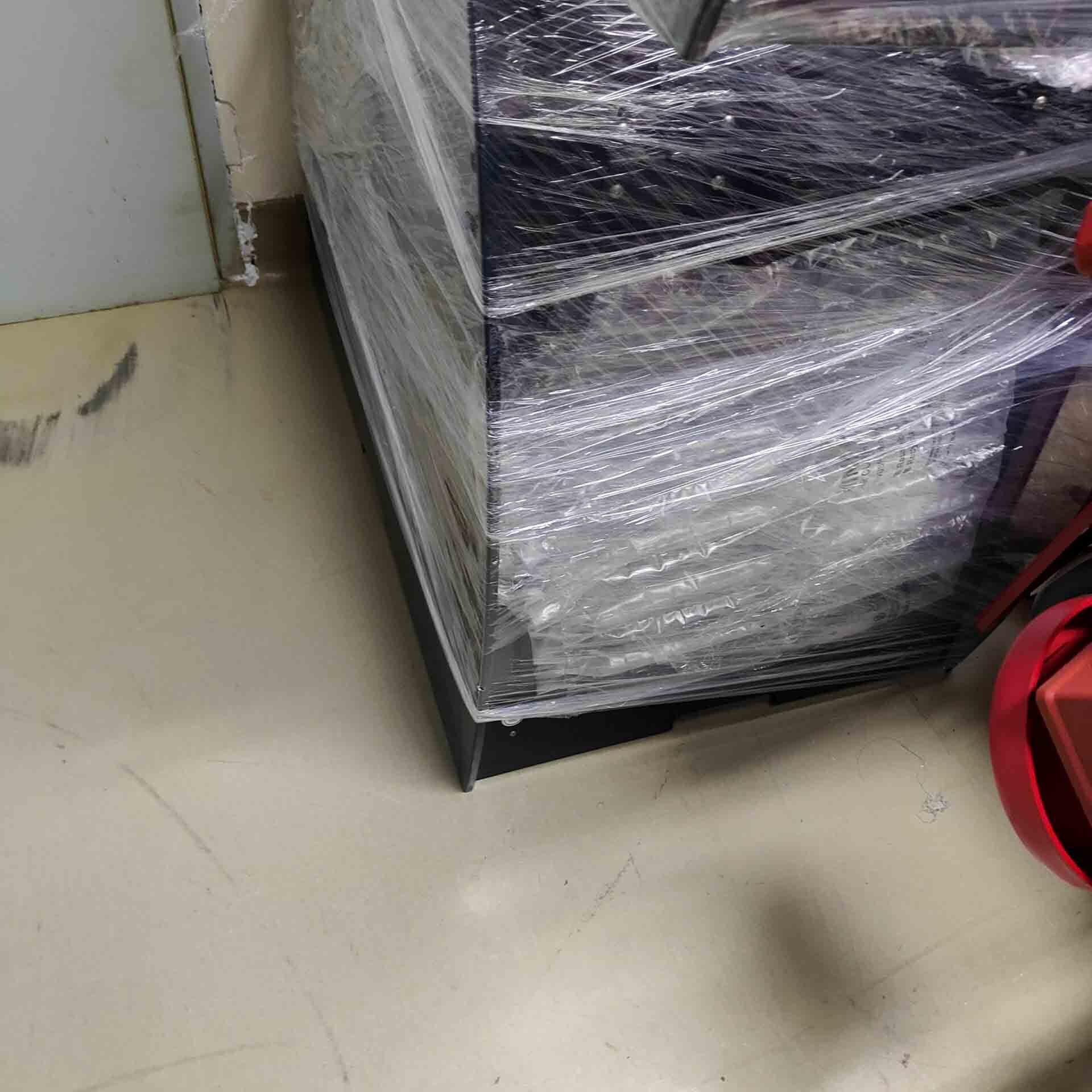
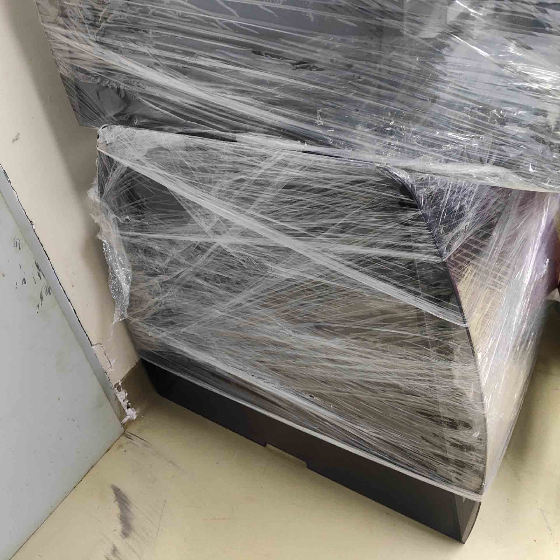
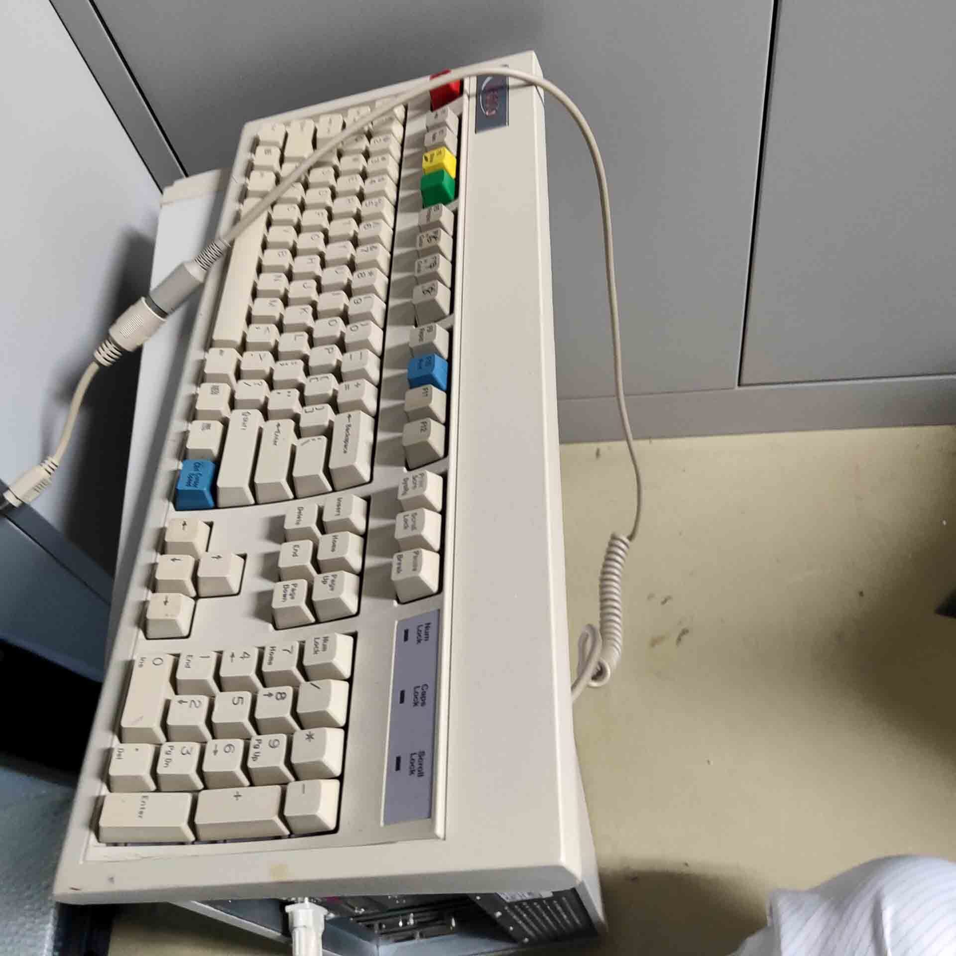
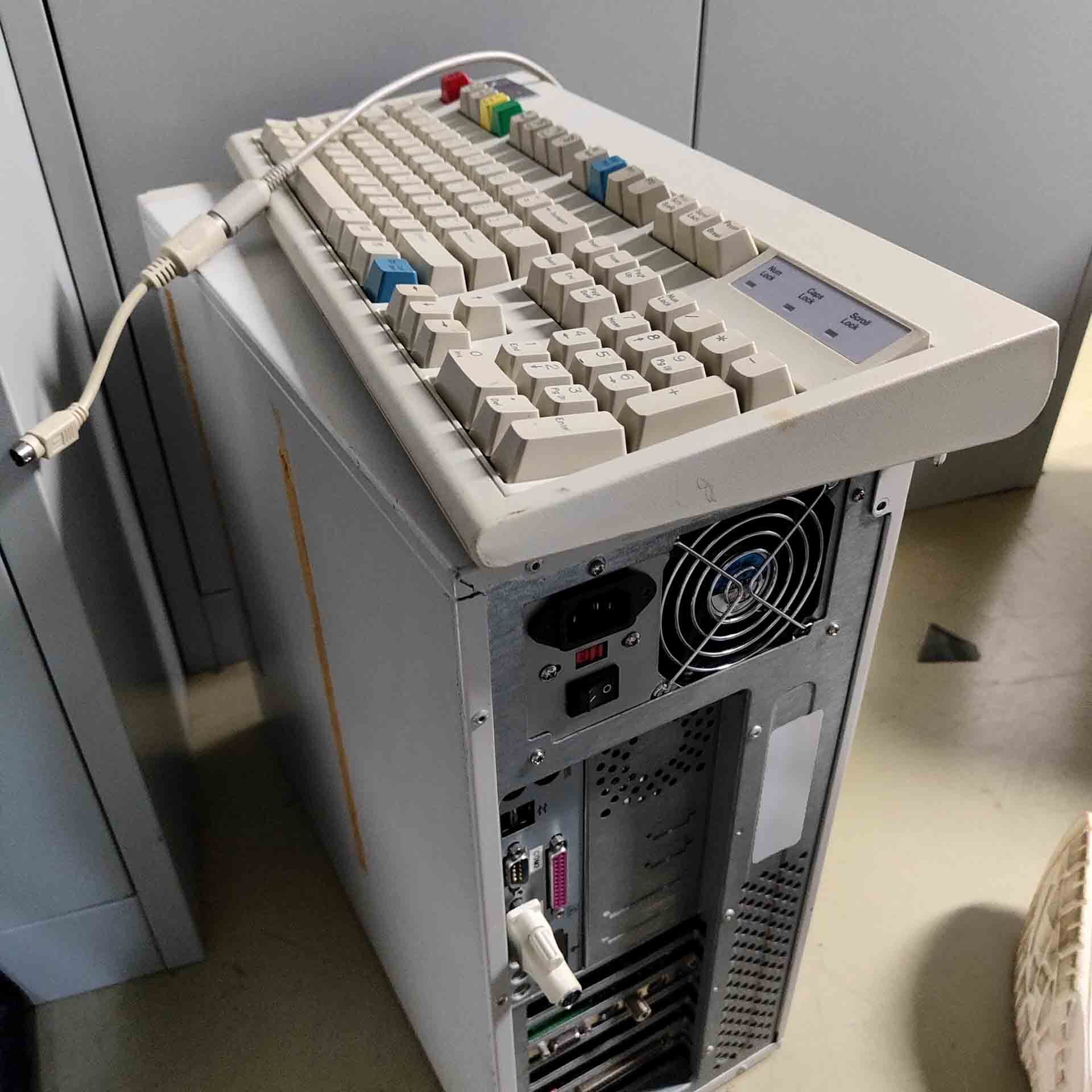
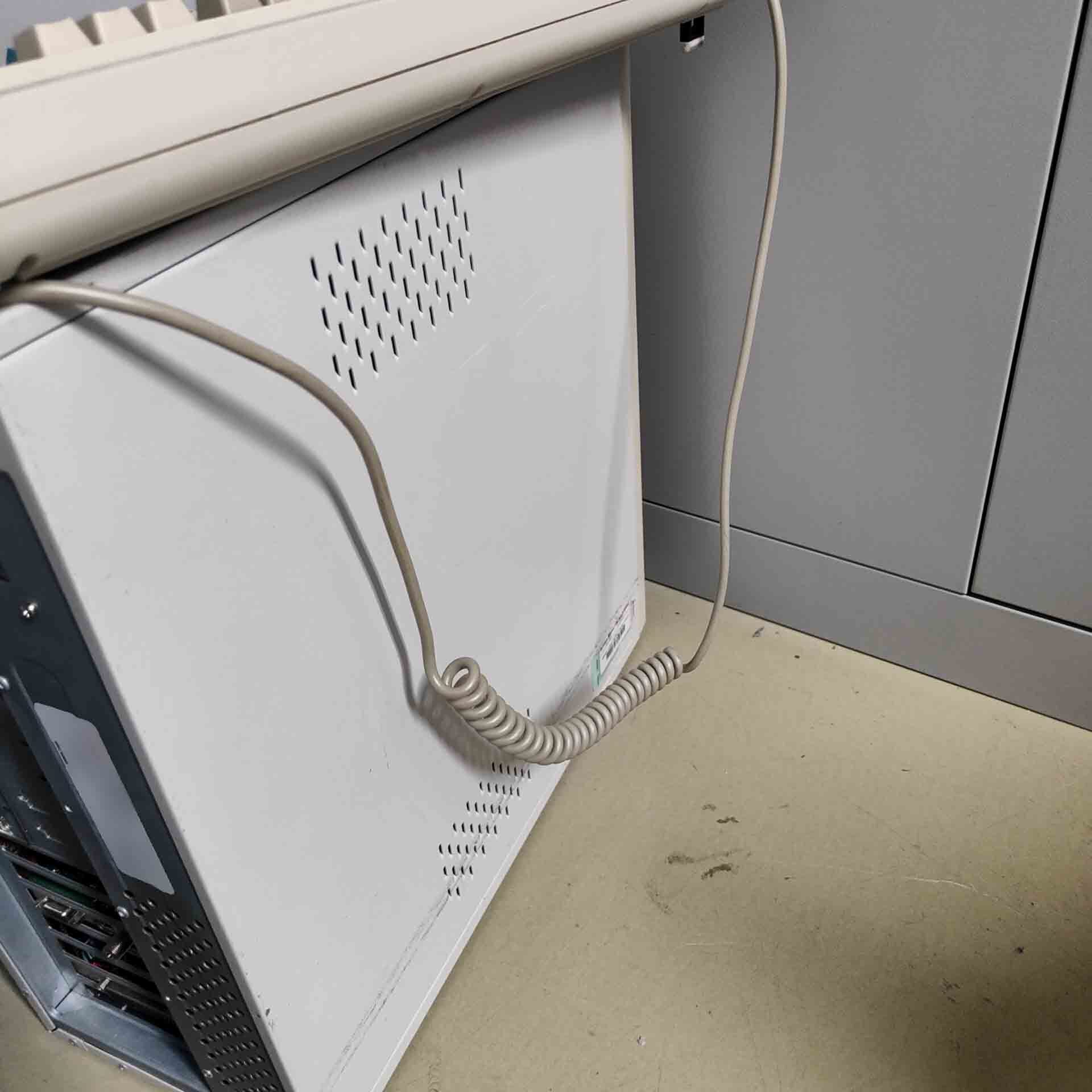
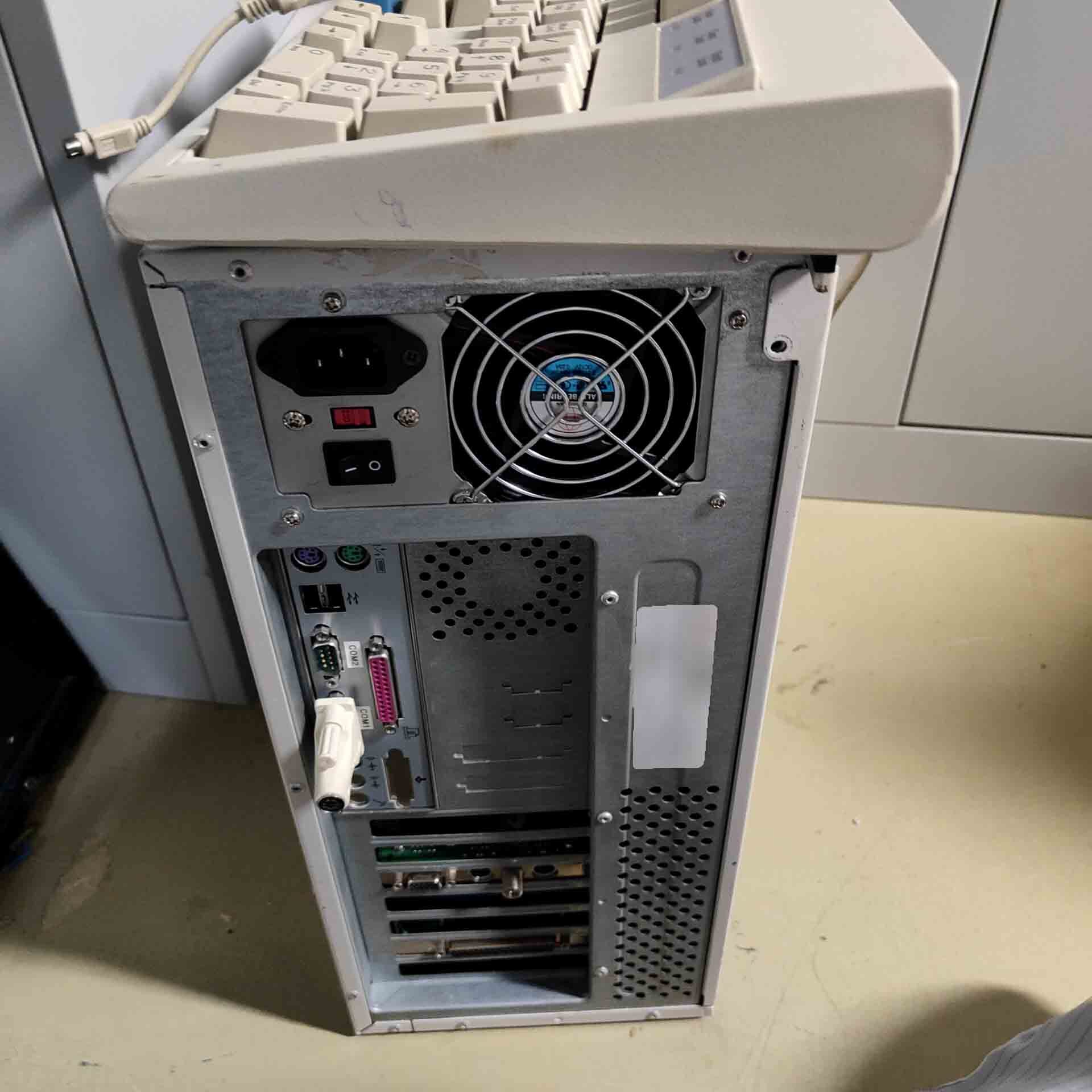
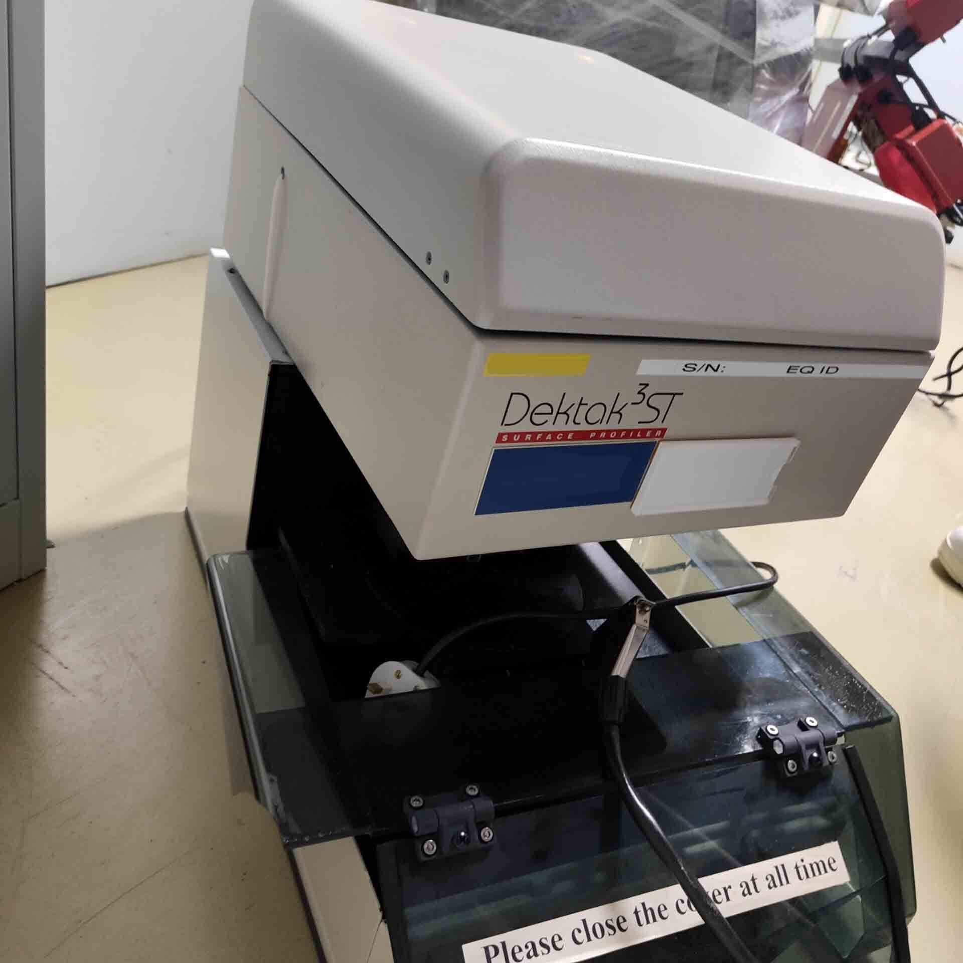
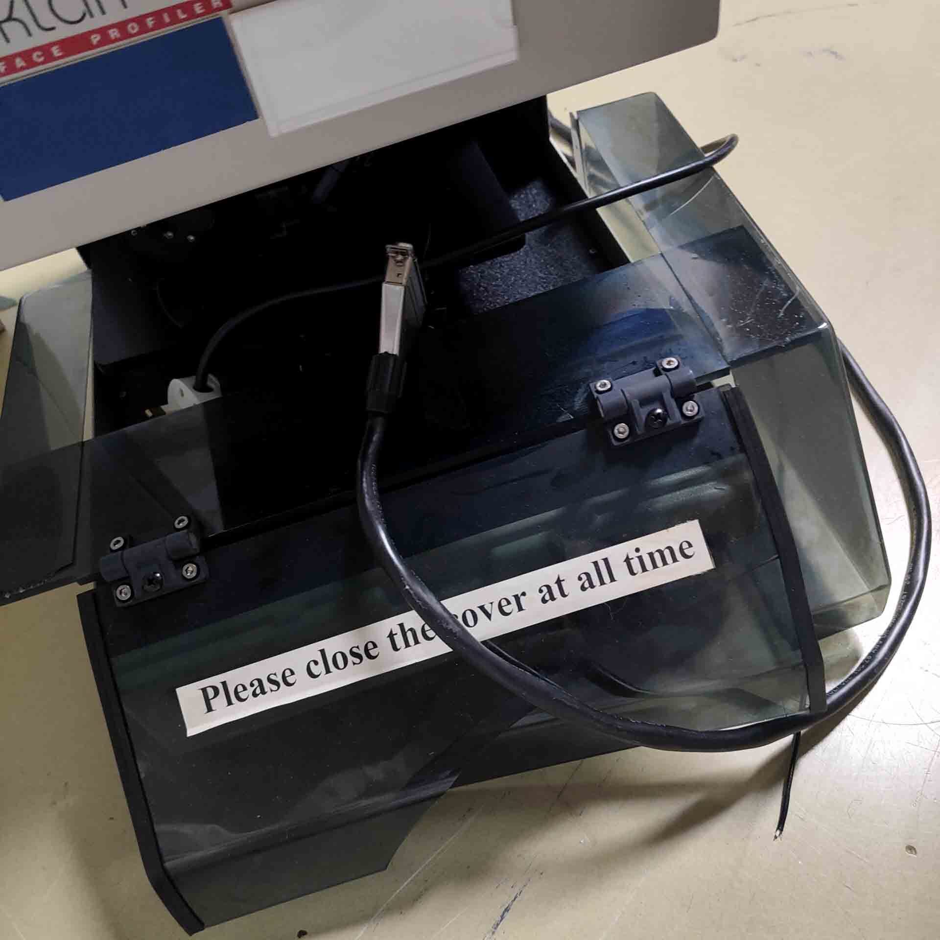
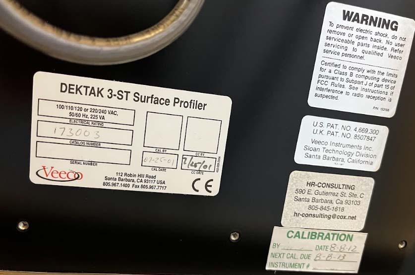
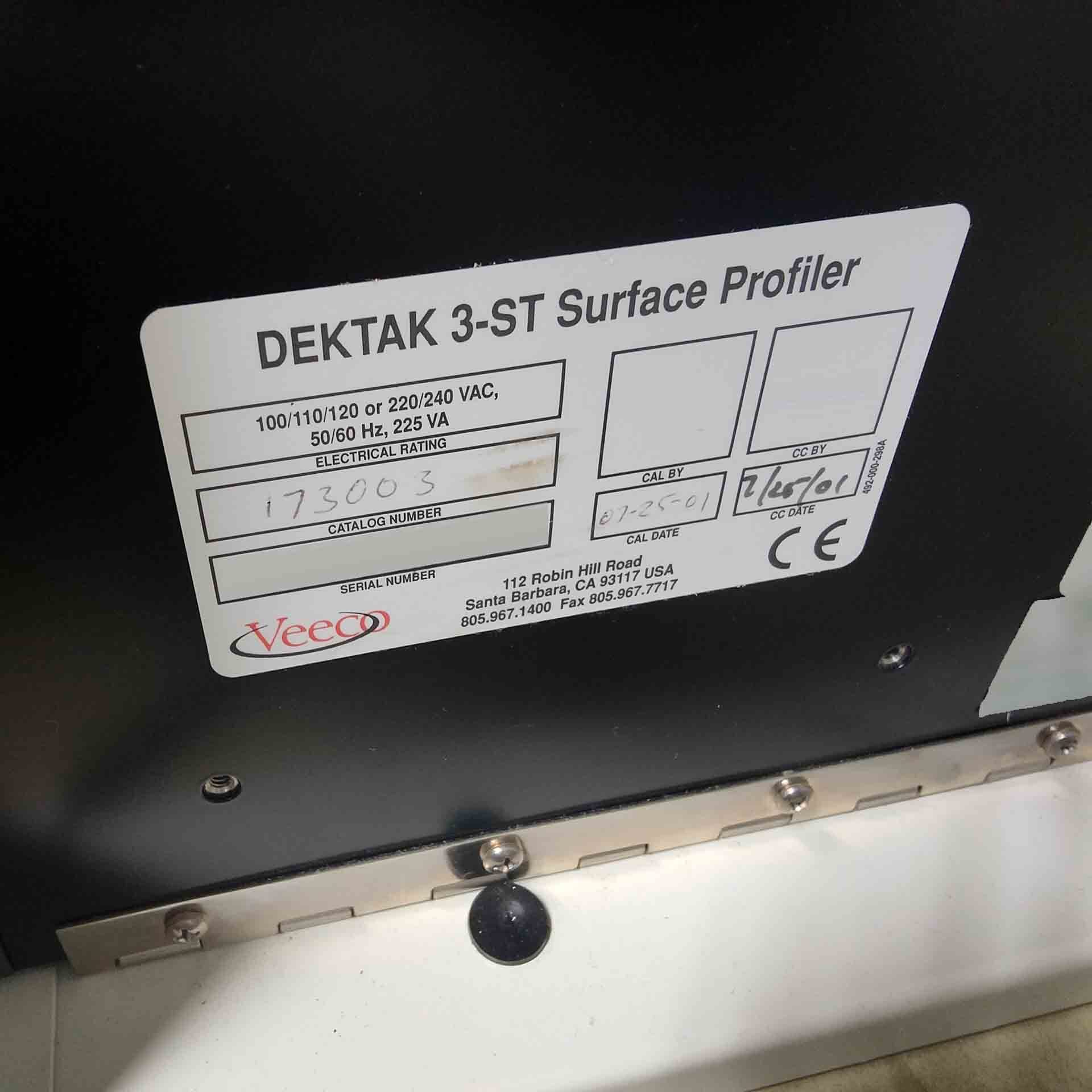
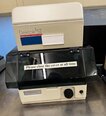
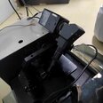
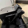
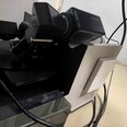
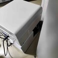
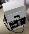
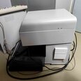
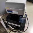
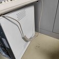
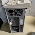
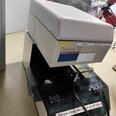
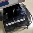
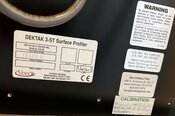
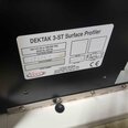
VEECO / SLOAN DEKTAK 3ST wafer testing and metrology equipment is an advanced platform that allows users to measure a variety of electrical, optical, and surface-related characteristics of semiconductor substrates. The system harnesses the power of Piezo-based surface profilometry to accurately measure surface topography and surface roughness at a high resolution of 1nm. It also offers advanced segmentation capabilities to profile thick resist or deep trenches. To improve precision, the unit uses a metrology device to stereoscopically measure and analyze semiconductor wafer parameters. VEECO DEKTAK 3ST also includes automated image acquisition of large surface areas on semiconductor substrates - helping enable more reliable products and more efficient production processes. Soft touch imaging enables improved imaging of sensitive surfaces and provides more accurate results with minimal force. Automated mapping capabilities enable computer-controlled scans of entire substrate surfaces in predetermined patterns, allowing for faster and more efficient analysis. SLOAN DEKTAK 3 ST's multi-axis stepper motor is capable of measuring substrates up to 8 inches in diameter and has advanced programmable/multi-step scan pattern capabilities. The machine also incorporates an intuitive graphical user interface with a set of on-screen icons enabling easy operation of the tool. Along with the wide range of features, the asset also allows the user to customize the wafer measurements with the ability to further tailor the measurement based on the given applications. It is designed for quick and easy calibration and maintenance, thereby allowing for trouble-free operation. A variety of additional features, including scratch detection and failure analysis capabilities, help make it suitable for both research and manufacturing environments. VEECO DEKTAK 3 ST is an advanced wafer testing and metrology model offering high accuracy and user flexibility to help drive improved product reliability and lower production costs. The equipment's automated mapping and imaging capabilities, intuitive graphical user interface and wide range of features make it well-suited for measuring a variety of characteristics in semiconductor substrates. The system can be used for a range of applications including defect detection, failure analysis, and device optimization.
There are no reviews yet